- 您现在的位置:买卖IC网 > Sheet目录3878 > PIC18F4610T-I/ML (Microchip Technology)IC MCU FLASH 32KX16 44QFN
PIC18F2X1X/4X1X
DS39636D-page 132
2009 Microchip Technology Inc.
14.1
CCP Module Configuration
Each Capture/Compare/PWM module is associated
with a control register (generically, CCPxCON) and a
data register (CCPRx). The data register, in turn, is
comprised of two 8-bit registers: CCPRxL (low byte)
and CCPRxH (high byte). All registers are both
readable and writable.
14.1.1
CCP MODULES AND TIMER
RESOURCES
The CCP modules utilize Timers 1, 2 or 3, depending
on the mode selected. Timer1 and Timer3 are available
to modules in Capture or Compare modes, while
Timer2 is available for modules in PWM mode.
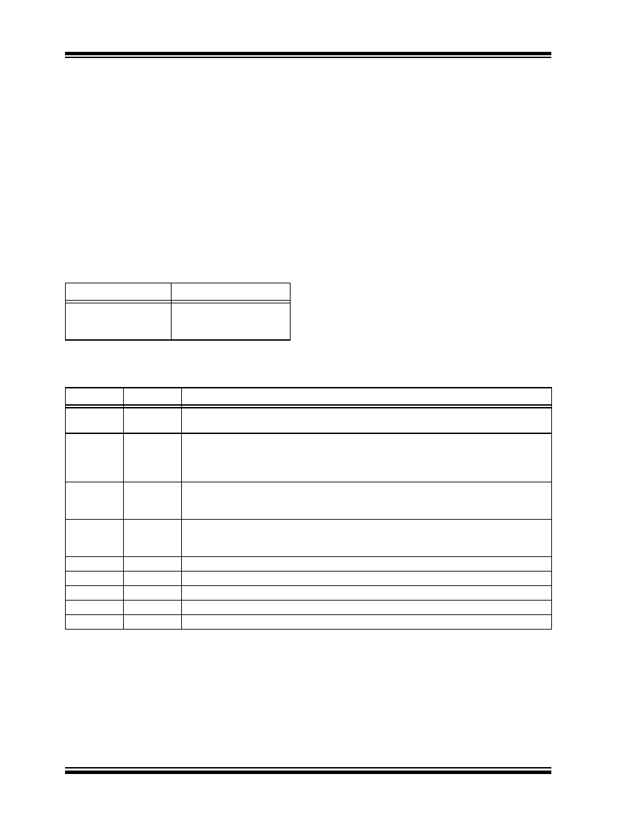
TABLE 14-1:
CCP MODE – TIMER
RESOURCE
The assignment of a particular timer to a module is
determined by the Timer-to-CCP enable bits in the
T3CON register (Register 13-1). Both modules may be
active at any given time and may share the same timer
resource if they are configured to operate in the same
mode (Capture/Compare or PWM) at the same time. The
interactions between the two modules are summarized in
Figure 14-1 and Figure 14-2. In Timer1 in Asynchronous
Counter mode, the capture operation will not work.
14.1.2
CCP2 PIN ASSIGNMENT
The pin assignment for CCP2 (Capture input, Compare
and PWM output) can change, based on device config-
uration. The CCP2MX Configuration bit determines
which pin CCP2 is multiplexed to. By default, it is
assigned to RC1 (CCP2MX = 1). If the Configuration bit
is cleared, CCP2 is multiplexed with RB3.
Changing the pin assignment of CCP2 does not auto-
matically change any requirements for configuring the
port pin. Users must always verify that the appropriate
TRIS register is configured correctly for CCP2
operation, regardless of where it is located.
TABLE 14-2:
INTERACTIONS BETWEEN CCP1 AND CCP2 FOR TIMER RESOURCES
CCP/ECCP Mode
Timer Resource
Capture
Compare
PWM
Timer1 or Timer3
Timer2
CCP1 Mode CCP2 Mode
Interaction
Capture
Each module can use TMR1 or TMR3 as the time base. The time base can be different
for each CCP.
Capture
Compare
CCP2 can be configured for the special event trigger to reset TMR1 or TMR3
(depending upon which time base is used). Automatic A/D conversions on trigger event
can also be done. Operation of CCP1 could be affected if it is using the same timer as a
time base.
Compare
Capture
CCP1 can be configured for the special event trigger to reset TMR1 or TMR3 (depending
upon which time base is used). Operation of CCP2 could be affected if it is using the
same timer as a time base.
Compare
Either module can be configured for the Special Event Trigger to reset the time base.
Automatic A/D conversions on CCP2 trigger event can be done. Conflicts may occur if
both modules are using the same time base.
Capture
PWM(1)
None
Compare
PWM(1)
None
PWM(1)
Capture
None
PWM(1)
Compare
None
PWM(1)
PWM
Both PWMs will have the same frequency and update rate (TMR2 interrupt).
Note 1:
Includes standard and Enhanced PWM operation.
发布紧急采购,3分钟左右您将得到回复。
相关PDF资料
PIC18F4610-E/PT
IC MCU FLASH 32KX16 44TQFP
PIC18F4610-E/ML
IC MCU FLASH 32KX16 44QFN
PIC18LF2331T-I/SO
IC MCU FLASH 4KX16 28SOIC
PIC18F4515T-I/PT
IC MCU FLASH 24KX16 44TQFP
PIC18F4431T-I/ML
IC MCU FLASH 8KX16 44QFN
PIC18F4431-E/ML
IC MCU FLASH 8KX16 44QFN
PIC18F4410T-I/ML
IC MCU FLASH 8KX16 44QFN
PIC18F4410-E/PT
IC MCU FLASH 8KX16 44TQFP
相关代理商/技术参数
PIC18F4610T-I/PT
功能描述:8位微控制器 -MCU 64KB 3968 RAM 36 I/O RoHS:否 制造商:Silicon Labs 核心:8051 处理器系列:C8051F39x 数据总线宽度:8 bit 最大时钟频率:50 MHz 程序存储器大小:16 KB 数据 RAM 大小:1 KB 片上 ADC:Yes 工作电源电压:1.8 V to 3.6 V 工作温度范围:- 40 C to + 105 C 封装 / 箱体:QFN-20 安装风格:SMD/SMT
PIC18F4620-E/ML
功能描述:8位微控制器 -MCU 64KB 3968 RAM 36 I/O RoHS:否 制造商:Silicon Labs 核心:8051 处理器系列:C8051F39x 数据总线宽度:8 bit 最大时钟频率:50 MHz 程序存储器大小:16 KB 数据 RAM 大小:1 KB 片上 ADC:Yes 工作电源电压:1.8 V to 3.6 V 工作温度范围:- 40 C to + 105 C 封装 / 箱体:QFN-20 安装风格:SMD/SMT
PIC18F4620-E/P
功能描述:8位微控制器 -MCU 64KB 3968 RAM 36 I/O RoHS:否 制造商:Silicon Labs 核心:8051 处理器系列:C8051F39x 数据总线宽度:8 bit 最大时钟频率:50 MHz 程序存储器大小:16 KB 数据 RAM 大小:1 KB 片上 ADC:Yes 工作电源电压:1.8 V to 3.6 V 工作温度范围:- 40 C to + 105 C 封装 / 箱体:QFN-20 安装风格:SMD/SMT
PIC18F4620-E/PT
功能描述:8位微控制器 -MCU 64KB 3968 RAM 36 I/O RoHS:否 制造商:Silicon Labs 核心:8051 处理器系列:C8051F39x 数据总线宽度:8 bit 最大时钟频率:50 MHz 程序存储器大小:16 KB 数据 RAM 大小:1 KB 片上 ADC:Yes 工作电源电压:1.8 V to 3.6 V 工作温度范围:- 40 C to + 105 C 封装 / 箱体:QFN-20 安装风格:SMD/SMT
PIC18F4620-E/PT
制造商:Microchip Technology Inc 功能描述:IC 8BIT MCU PIC18F 40MHZ TQFP-44 制造商:Microchip Technology Inc 功能描述:IC, 8BIT MCU, PIC18F, 40MHZ, TQFP-44
PIC18F4620-I/ML
功能描述:8位微控制器 -MCU 64KB 3968 RAM 36 I/O RoHS:否 制造商:Silicon Labs 核心:8051 处理器系列:C8051F39x 数据总线宽度:8 bit 最大时钟频率:50 MHz 程序存储器大小:16 KB 数据 RAM 大小:1 KB 片上 ADC:Yes 工作电源电压:1.8 V to 3.6 V 工作温度范围:- 40 C to + 105 C 封装 / 箱体:QFN-20 安装风格:SMD/SMT
PIC18F4620-I/P
功能描述:8位微控制器 -MCU 64KB 3968 RAM 36 I/O RoHS:否 制造商:Silicon Labs 核心:8051 处理器系列:C8051F39x 数据总线宽度:8 bit 最大时钟频率:50 MHz 程序存储器大小:16 KB 数据 RAM 大小:1 KB 片上 ADC:Yes 工作电源电压:1.8 V to 3.6 V 工作温度范围:- 40 C to + 105 C 封装 / 箱体:QFN-20 安装风格:SMD/SMT
PIC18F4620-I/P
制造商:Microchip Technology Inc 功能描述:IC 8BIT FLASH MCU 18F4620 DIP40